Publisher: Supplier of LED Display Time: 2021-12-29 15:31 Views: 684
1 LED chip type
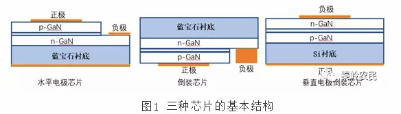
From the structural point of view, the types of LED chips are mainly divided into three categories: horizontal electrode chips, flip chips and vertical electrode chips.
As shown in Figure 1 below
2 LED packaging
Packaging is an intermediate link necessary to realize the LED from the chip to the final product. The function of the package is to provide sufficient protection for the chip to prevent the chip from being exposed to the air for a long time or from mechanical damage and failure, so as to improve the stability of the chip; For LED packaging, It also needs to have good light extraction efficiency and good heat dissipation. A good package can make the LED have better luminous efficiency and heat dissipation environment, thereby improving the life of the LED.
The function of the package: to realize the function of inputting electrical signals, protecting the normal operation of the chip, and outputting visible light.
3 Commonly used LED chip packaging forms
1) Leaded package
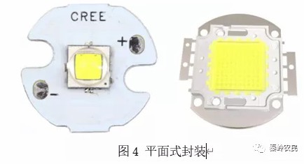
2) Flat package
3) Surface mount package
4) Piranha package
5) Power package
4-pin package structure
LED pin-type packages use lead frames as the pins of various package appearances. It is the first package structure to be successfully developed and put on the market. There are many varieties and high technology maturity. The internal structure and reflective layer of the package are still being improved.
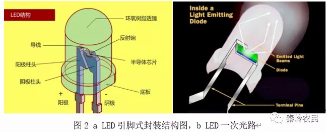
The LED chip is bonded on the lead frame. The positive electrode is connected to a support with a gold wire, and the negative electrode is connected in the reflector cup of the support with a gold wire or directly bonded in the reflector cup of the support with silver paste. The top is encapsulated with epoxy resin to make a cylinder + hemisphere type. The shape of the epoxy resin acts as a lens to control the divergence angle of the beam. At the same time, the refractive index of epoxy resin plays a role in the transition between the chip and the air, which improves the luminous efficiency of the chip. The refractive index of the chip is high and the angle of total reflection to air is small. For epoxy resin, the angle of total reflection is increased, which can make more More light output.
Generally, the size of this kind of LED chip is 0.25mmX0.25mm, the radius of the packaged element is 5mm, the luminous power is 1~2 lumens, and the working current is 20~30mA. Traditional small chip LEDs have limited their applications because of their low luminous power. Most of them are used for display or indication. For example, the indicator light of the instrument.
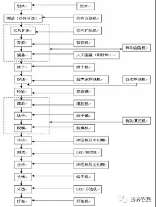
4.1 Lead package process
5 Flat package
Planar packaging is a combination of multiple LED chips into a planar structural package. Through the proper connection of LEDs (series and parallel) and appropriate optical structure, the light-emitting segments and light-emitting points of the light-emitting display can be formed, and then these light-emitting segments and light-emitting points form various light-emitting displays, such as digital tubes and "meter"-shaped tubes And matrix tube, etc.
Take the Xlamp XP-E product of American Cree company as an example. It adopts a packaging manufacturing process with higher production efficiency. Ceramics are used as the packaging substrate. The product units are on a ceramic substrate in a planar shape and arranged in an array. Together. Mount the chip on each substrate unit, and then encapsulate a layer of silica gel on the ceramic substrate to form the required optical lens structure. Its structure includes ceramic substrates, new products, Au wires and plastic encapsulated silica gel, etc.
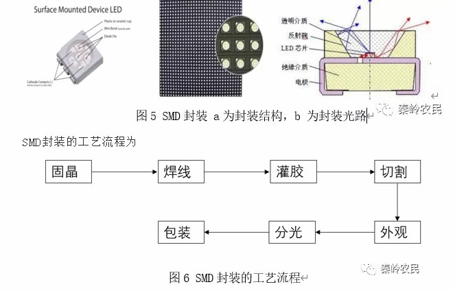
6 Surface Mount Package (SMD)
Surface mount package (SMD) is a new type of surface mount package. It has the advantages of small size, large scattering angle, good luminous uniformity, and high reliability. The light-emitting color can be a variety of colors including white light, which is very suitable for keyboard display lighting of mobile phones, backlight lighting of TV sets, and electronic products that require lighting or instructions. In recent years, SMD packaging has become large-sized and high-power The development direction, three or four Led chips are encapsulated in one patch, which can be used to assemble lighting products.
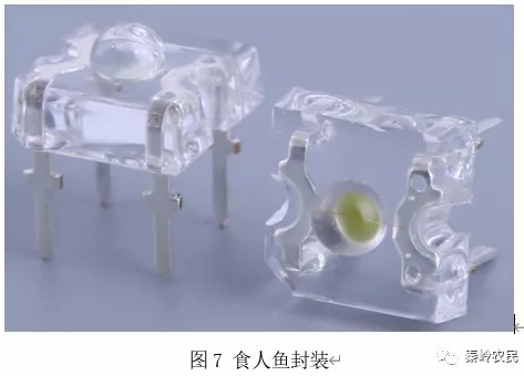
7 Piranha Package
The piranha package is square and uses a transparent resin package. Because its shape is very similar to the Piranha in the Amazon, it is called a piranha package. It has four pins, and there is a missing pin at the negative pole. Piranha is an astigmatic LED with a light-emitting angle greater than 120 degrees, high luminous intensity, and can withstand greater power. Because the bracket used by the Piranha LED is made of copper and has a large area, heat transfer and heat dissipation are fast. After the LED is lit, the heat generated by the PN junction can quickly pass from the four legs of the bracket to the copper strip of the PCB.
Piranha encapsulation steps
1) Select the bracket of Piranha LED
2) Cleaning the bracket
3) Determine the shape, size and depth of the concave bowl in the bracket
4) The LED chip is fixed in the holder bowl
5) Drying
6) Two-stage welding of LED chips
7) Selection of mold pellets
8) Glue in the mold
9) The bracket of the soldered LED chip is placed upside down in the die
10) Drying, demoulding and cutting
11) Testing and sorting
8 power package
With the increase of LED chip input power, it has brought about large heat generation and high light extraction efficiency, which puts forward newer and higher requirements for LED packaging technology, making power LED packaging technology a research hotspot in recent years. Power LED is also the core of future semiconductor lighting.
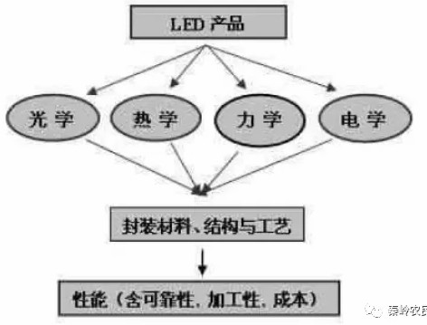
The high-power LED package design is shown in Figure 1 in terms of light, electricity, heat, structure and technology. Specifically, the key technologies of packaging include
8.1 Geothermal resistance packaging process
Mainly include chip layout, packaging material selection and process, heat sink design, etc. The thermal resistance of LED packaging mainly includes internal thermal resistance of the material and interface thermal resistance. The role of the heat dissipation substrate is to absorb the heat generated by the chip and conduct it to the heat sink to achieve heat exchange with the outside world. Commonly used heat dissipation substrate materials include silicon, metals (aluminum, copper), ceramics (such as Al2O3, AlN, SiC) and conforming materials. The package interface also has a great influence on the thermal resistance. If the interface is not handled correctly, it is difficult to obtain a good heat dissipation effect. Therefore, the selection of the thermal interface material between the chip and the heat dissipation substrate is very important. LED packaging using low temperature or eutectic solder, tin paste or nano-particle-doped conductive silver glue as the interface material can greatly reduce the interface thermal resistance.
8.2 High light extraction rate packaging structure and process
The loss of photons generated by the chip's luminous radiation when emitted mainly includes three aspects: 1) the internal structure of the chip and the absorption of materials; 2) the reflection loss of the photon at the exit interface due to the difference in refractive index; 3) due to The incident angle is greater than the total reflection loss caused by the critical angle of total reflection. By coating a transparent glue layer (potting glue) with a relatively high refractive index on the surface of the chip, the glue layer is between the chip and the air, which effectively reduces the loss of photons at the interface and improves the light extraction efficiency.
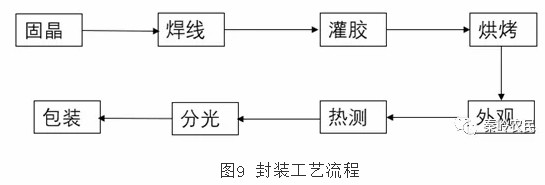
8.3 Packaging process


Shenzhen LCF Technology Co., Ltd.
Support Hotline
400-618-8884 / 0755-66833488(+86)187-0755-0636
Company Address
LCF Sound & Optoelectronics Industry Park, Gushu, Bao'an District, Shenzhen.
Copyright © 2004-2024 LCF LED Display Screen All rights reserved. Guangdong ICP 15089785-3 Subsidiaries: Dongguan Tongdachuang Industrial Co., Ltd., Anshun Lianshunda Technology Co., Ltd. (holdings)